December 6, 2021

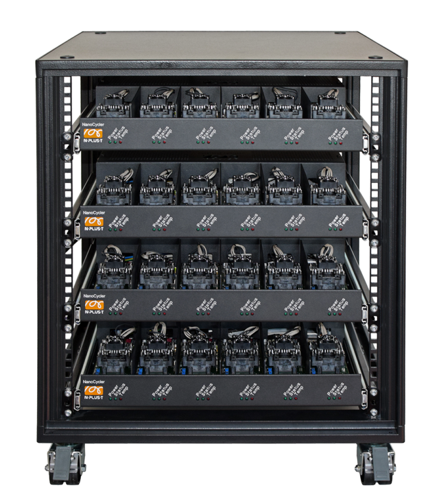
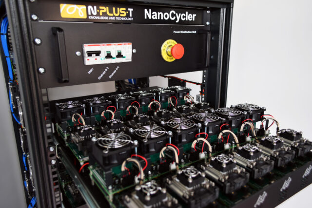
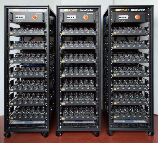
NplusT delivered 3 large size NanoCycler HS equipment to an important Chinese customer.

Based on its innovative architecture, the system allows to execute up to 252 fully independent tests, including package level thermal control, on NAND memories at the same time. The communication speed with the devices under test reaches 1.6 GT/sec on two channels in parallel, with zero-overhead pattern generation and pattern matching.

These equipments – being able to test the latest and future generation of NAND devices – aim at enhancing the customer’s development flow in the implementation of data centers and high-performance storage applications.

Tamas Kerekes, President and CEO of NplusT declared: “When building the equipment, we had to face the serious challenge of the component shortage. Our engineering team provided an excellent answer: the necessary design changes further improved system performance. We have been able to design, qualify, manufacture and test in a really short time. Now, our expectation is to see our customer executing efficiently their characterization and sorting tasks, we will provide them all necessary support. The delivery of these equipment also represents an important milestone to increase our presence in China, which is our fastest growing market today.”

November 24, 2020

The speed and complexity of the latest TLC and QLC flash technologies set new challenges in designing large capacity high performance SSD devices, from the hardware (signal integrity, power management) and the firmware (flash algorithms, error correction) point of view. Massive amounts of accurate data must be collected and analyzed to characterize the flash endurance, errors, defects, operation’s timing and power.
NanoCycler HS, bundled with BarnieMAT data analytics, provides the best-in-class and most cost effective solution for the exploration of the NAND memories.

NanoCycler HS:

Supports endurance and functional testing of NAND devices by providing C++ and Python API with full ONFI command set and with customizable signal sequences.

Exercises and stresses at-speed – up to 1.6 GT/sec – the devices under test faithfully replicating the use conditions of the application.

Provides high-accuracy – 10 mV precision – programmable power supplies for accurate voltage margins analysis.

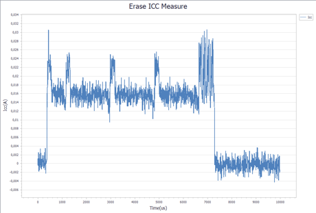
Captures the power consumption for each supply at 50 nsec sampling rate with 1 mA resolution. Flash operations power consumption data are processed in real time to provide high resolution current consumption traces, and key metrics (peak, average, distributions) over long period of time.

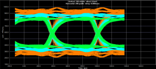
Characterizes the flash interface timing with 1 nsec I/O edge placement and 20 nsec flash response time acquisition.

Has a scalable and expandable architecture, from 1 to 48 test sites, to optimize cost and long term investment.

Allows full independence of the test sites where each device under test can run at individual temperature, timing, voltage levels, with different test programs.

Integrates the data analysis environment to post-process and present the results to accelerate time to product.

Highest quality characterization results at the lowest cost and effort – NanoCycler HS represents a future-safe investment to design high-performance reliable mass storage devices.


November 20, 2019

NplusT is participating in the 2nd open call for Value Chain Oriented and Interdisciplinary Technology Transfer Experiments in the framework of TETRAMAX, the #1 innovation hub for digitizing European industries in the domain of customized and low-energy computing (CLEC).

Tamas Kerekes presented the technology transfer project “HS-CHAR: High Speed Characterization of Mass Storage Devices”, which is being developed together with PCB Design, during the annual TETRAMAX Partners Meeting, held in Aachen on September 26.

TETRAMAX is proving to be a very efficient vehicle to promote small size projects, as Tamas said:

“Let me share you about my experience and consideration about the TETRAMAX projects and in particular about the call related to the bilateral technology transfer.

My company is a small SME working in the semiconductor/electronics industry. We spend more than half of our engineering resources on R&D. Even so, we cannot develop all technology we need by ourselves and we need to access technology of others. Contributions of national and EU funding are extremely useful to support our business growth. There are many calls and opportunities. On the other hand, we don’t have all resources to monitor and select the calls, even less to write many applications (a typical Sunday night task). So we need to focus on the opportunities where either: 1) the success rate is very good and the funded amount is high or: 2) the preparation of the application requires a reasonable amount of work. In both cases, the fast turnaround time (from application to final reporting and cashing) has to be short.

From this point of view, I consider TETRAMAX our best experience:

  • We have been advised about the opportunity by a TETRAMAX partner, without the need to monitor and study.
  • The preparation of the application is easy – of course once we have the content. We need to provide only the important data in a condensed way. I think this is a winning approach from the evaluation side as well.
  • The contracting procedure is easy again.

I warmly suggest TETRAMAX to other SMEs and I hope it will be a long success story!”


March 5, 2019

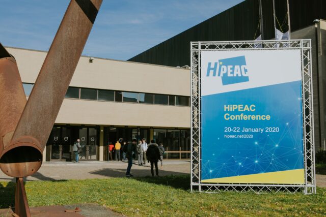
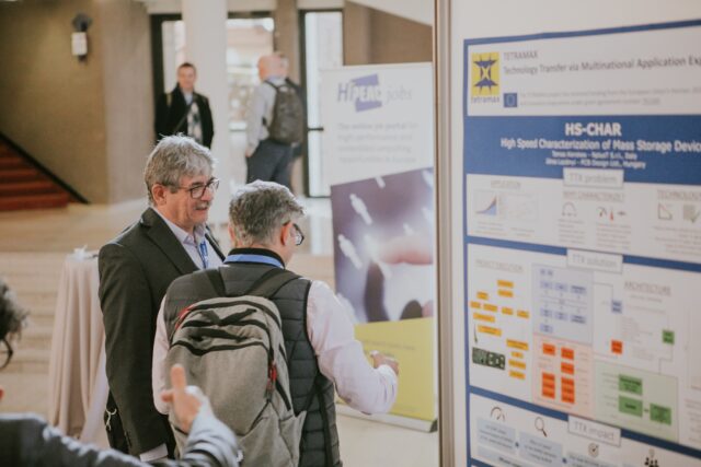
NplusT took part in the TETRAMAX poster session held at the 2020 edition of HiPEAC, the main European forum for experts in computer architecture, programming models, compilers and operating systems for embedded and general-purpose systems, attracting over 500 delegates each year.

The poster session showcased the projects funded in the framework of the European “Smart Anything Everywhere (SAE)” initiative, in the domain of customized low energy computing (CLEC) for CPS and the IoT, including the “HS-CHAR: High Speed Characterization of Mass Storage Devices” technology transfer project carried out by NplusT and PCB Design and devilered in December 2019.

The results of the “HSCHAR” project contributed to upgrade NplusT’s technology for NAND characterization, paving the way for the forthcoming release of NanoCycler High Speed, the best-in-class and most cost effective solution for the exploration of the NAND memories.


Legal Office

Loc. Castelfranco 132
05026 Montecastrilli
Terni, Italy

+39 075 5714845

info@n-plus-t.com

Laboratories

Via Donatella 12
06132 San Martino in Campo
Perugia, Italy

Capitale Sociale (Paid-up Capital) € 121.000,00 I.V.
Cod. Fisc. / Partita IVA (Vat Number) 00702760554
Sede CCIAA / n. REA : TR / 69772, PG / 272888
Iscriz. Reg. Imprese TR n. 00702760554


Privacy